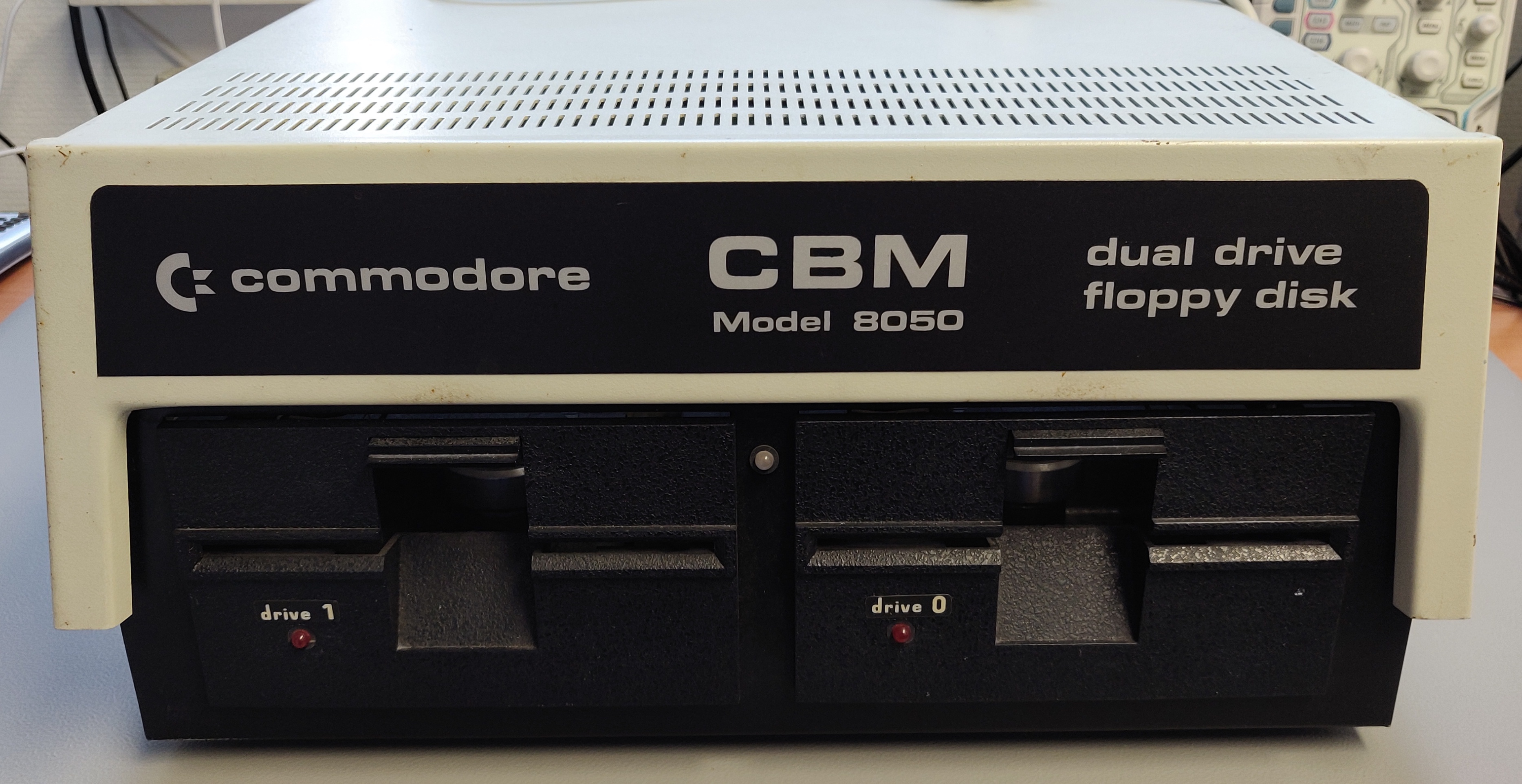
Commodore 8050
This Commodore dual floppy drive belongs to a customer. When I received it, it wouldn't power on at all.
Work done:
- Removed suppression capacitor
- Replaced power cable
- Diagnosed zero-page issue
- Replaced ROM
- Cleaned and lubricated drives
- Tested capacitors
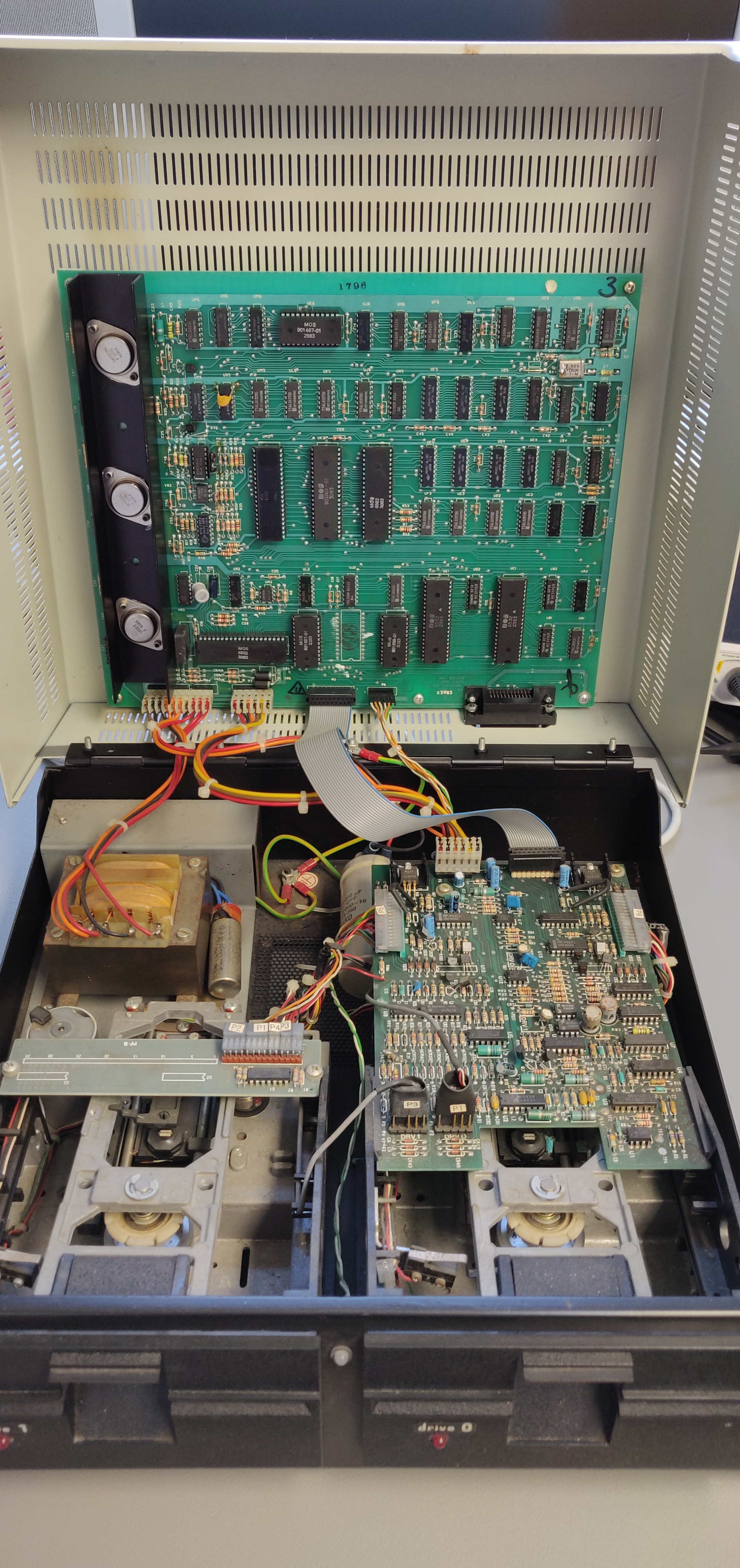
Interior inspection:
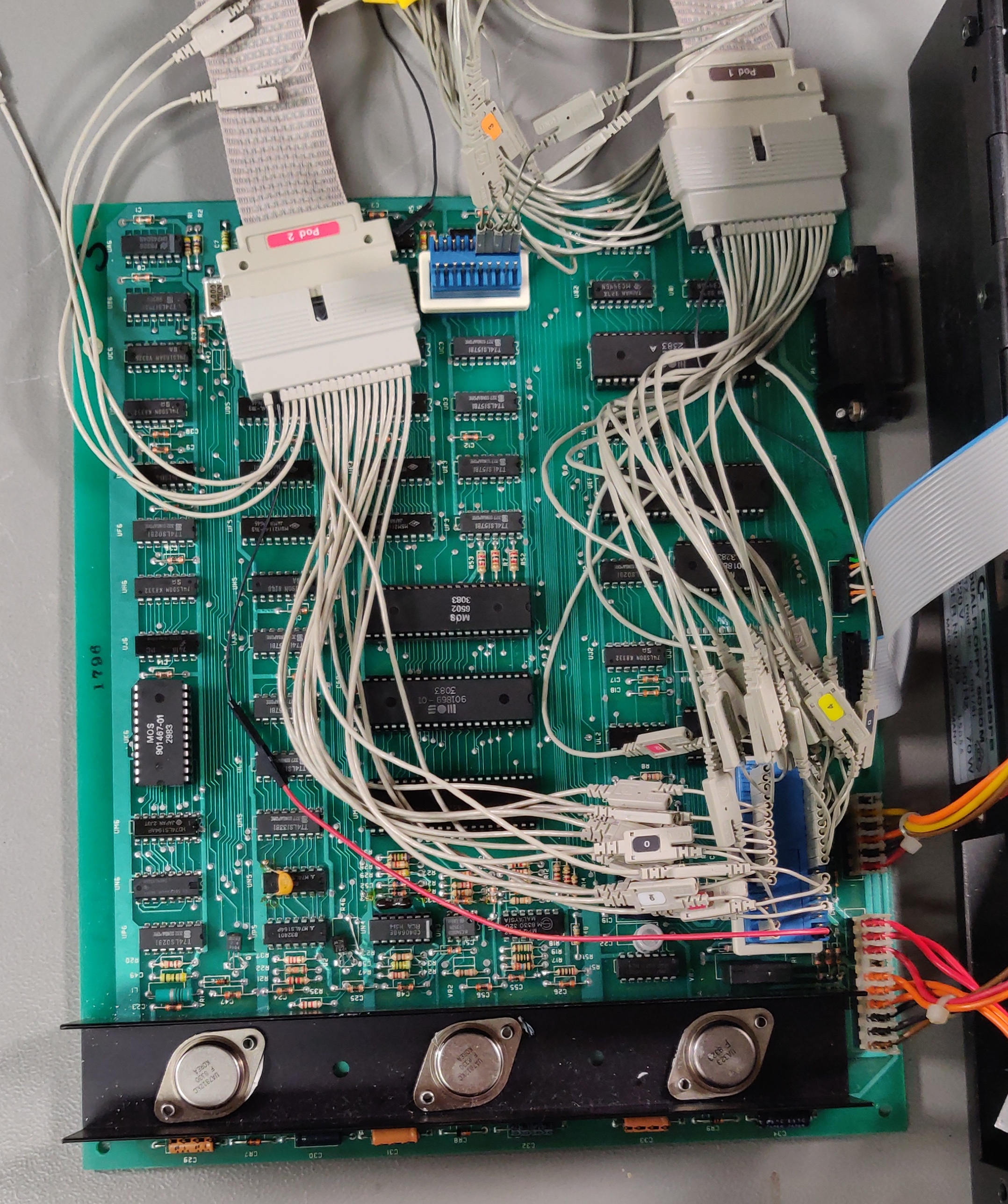
Opening this machine is truly a sight to behold, when you raise the lid it shows a large logic board attached to it. The circuit is quite complex, especially for a floppy drive:
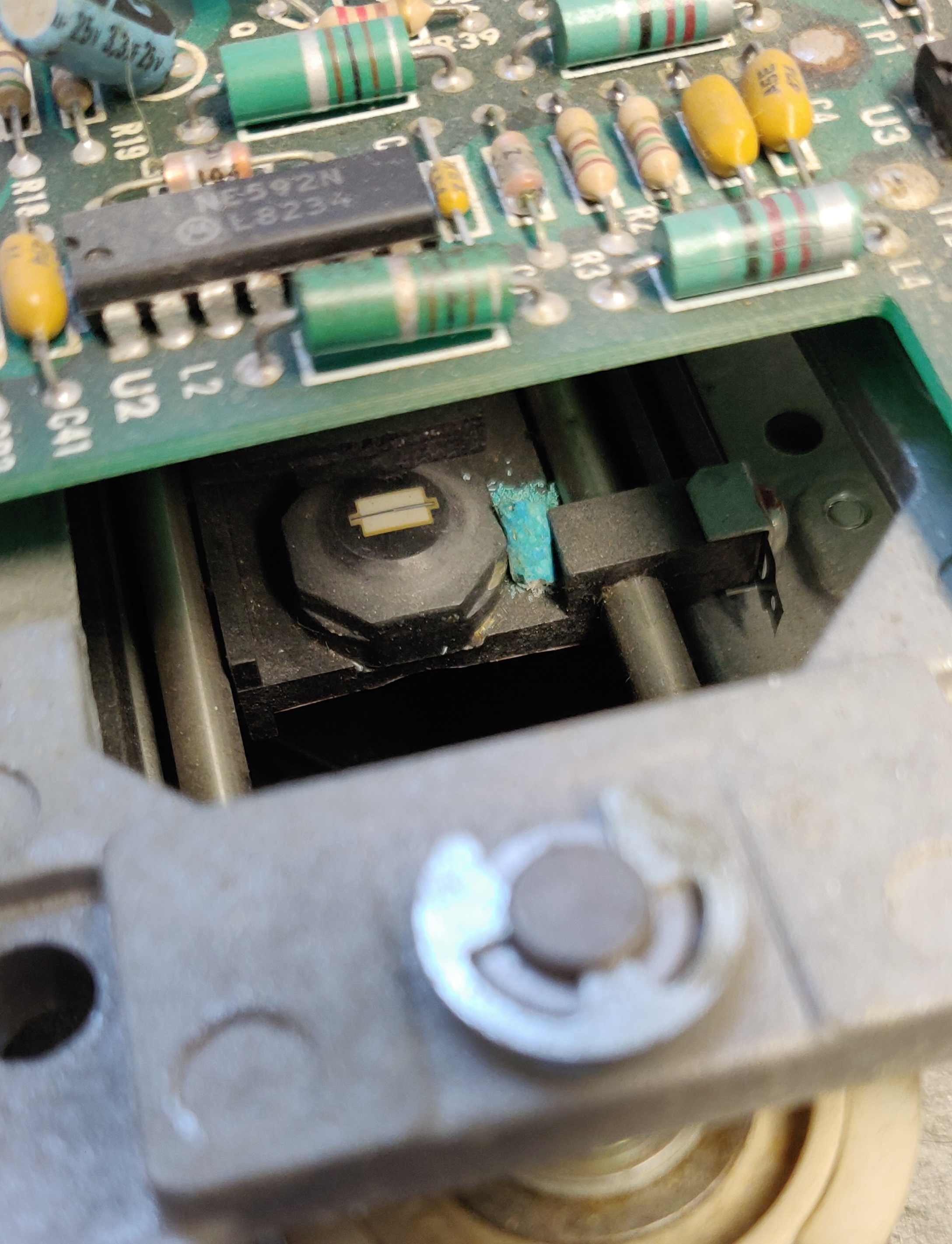
The main logic board uses two 6502 CPUs (twice the amount as the Commodore PET itself), three ROMs and several specific chips to interface with the analogue boards and the IEEE-488 interface to the PET.
Drive 0 has the analogue board attached to it, which is responsible for controlling the drives and converting the analogue magnetic flux information to binary data.
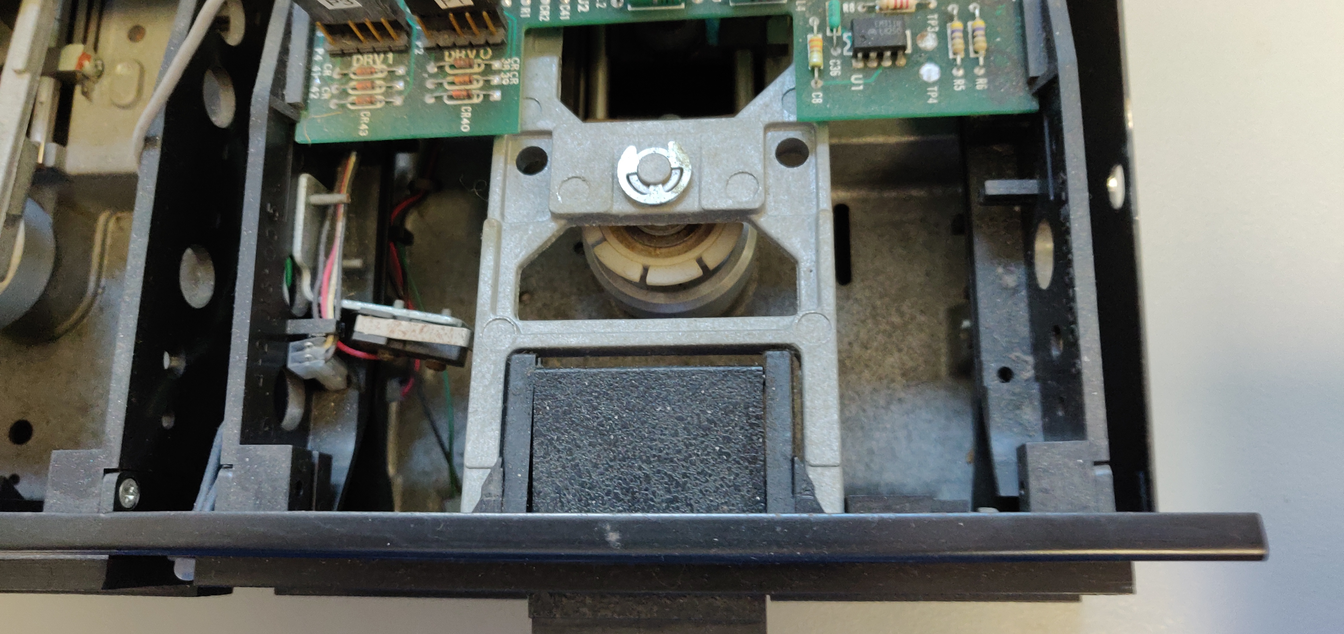
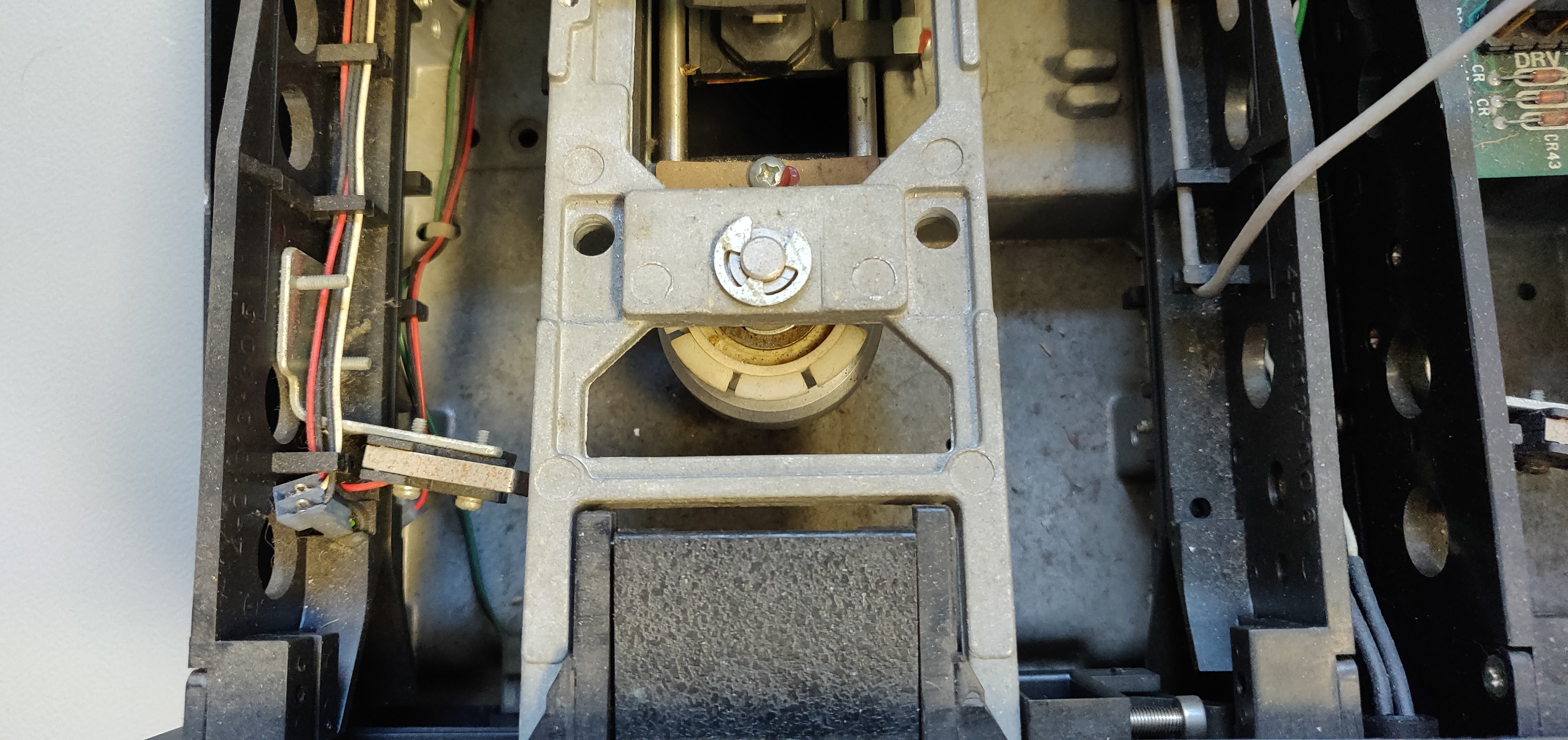
On the inside the drives were very dirty, and I found quite a few pellets of mouse / rat poison:
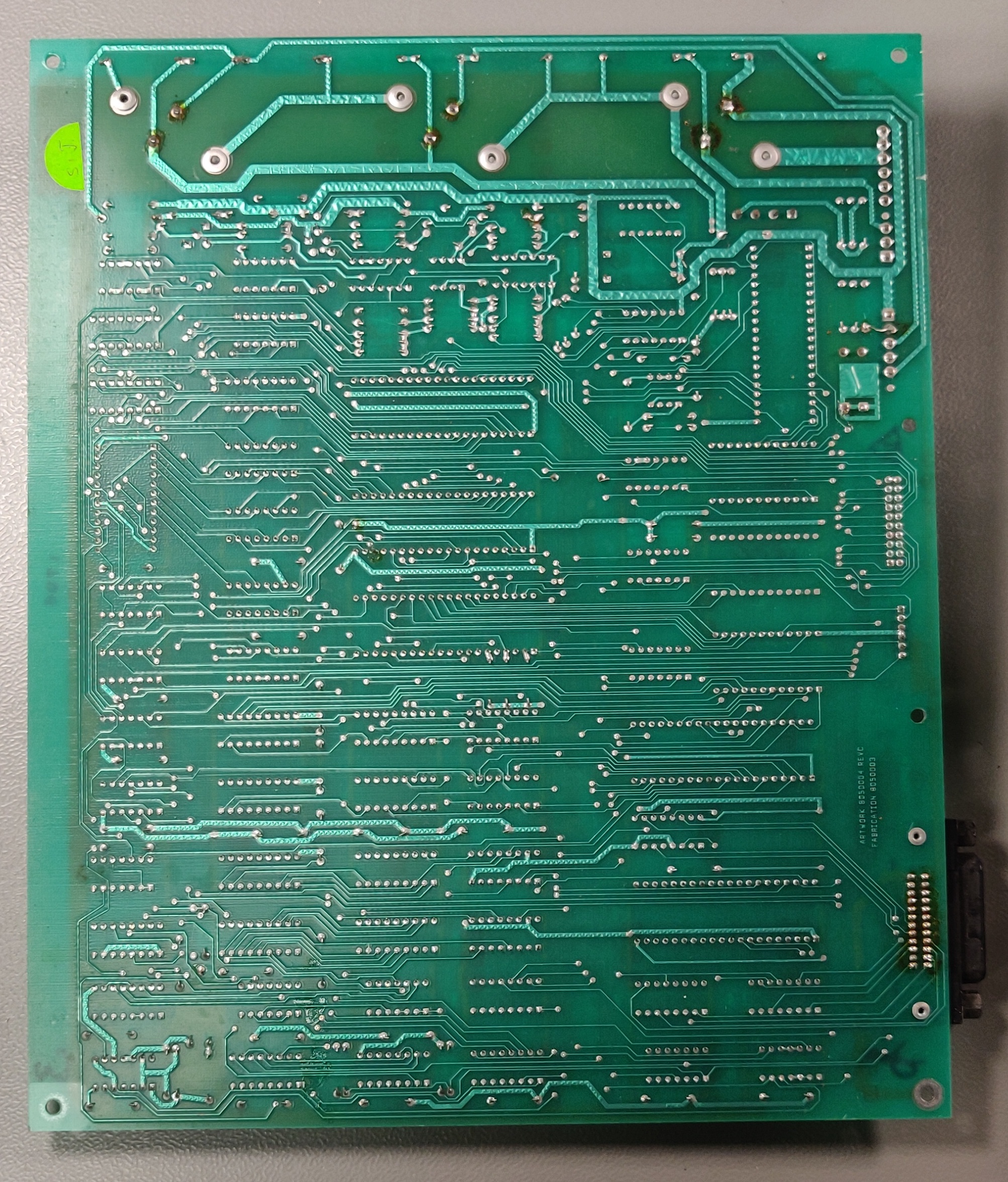
Here is a picture of the bottom of the logic board:
Initial power on
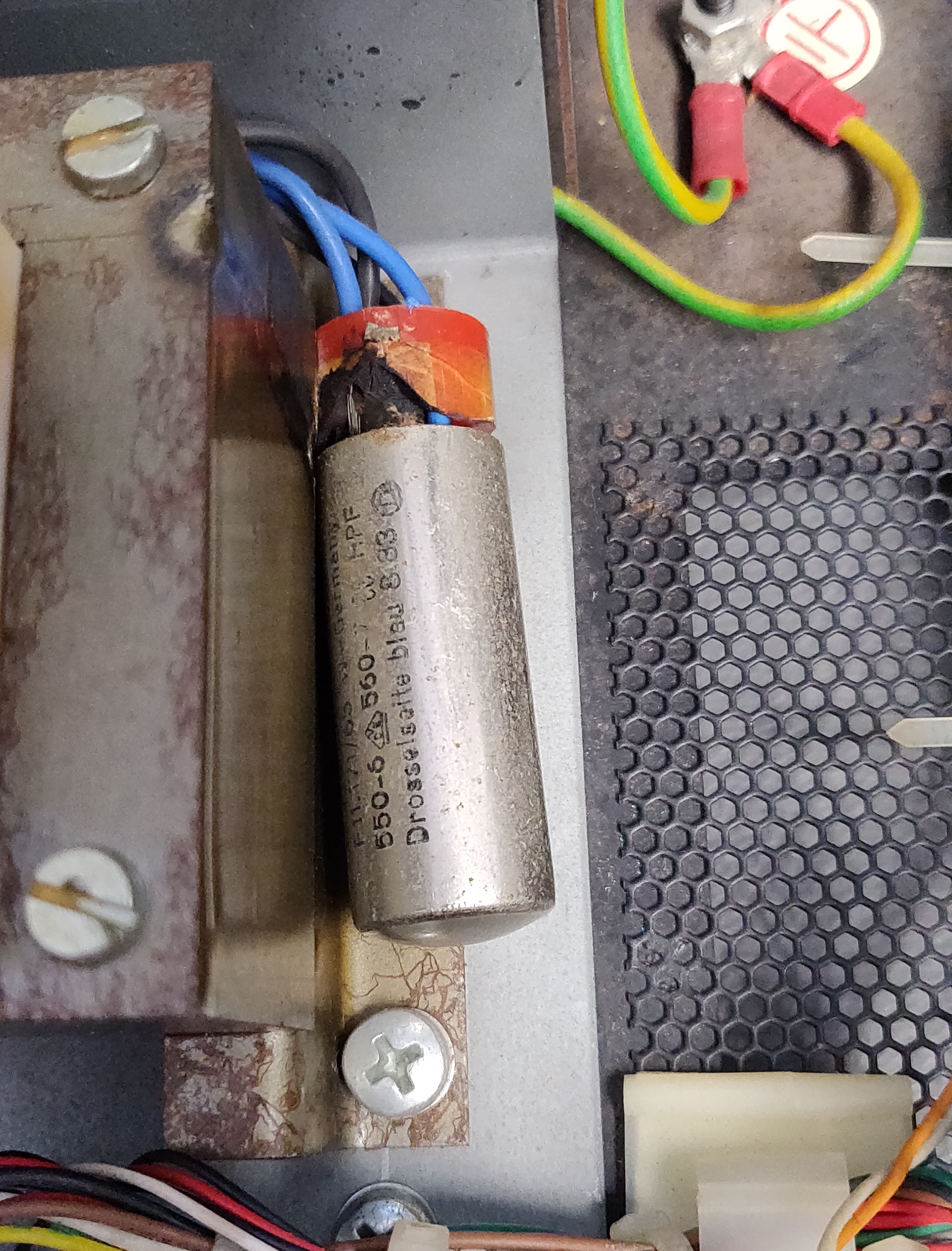
After I opened it up, it was soon clear why it wouldn't power on at all. There is a suppression capacitor installed, meant to reduce emissions back to the grid, which had blown:
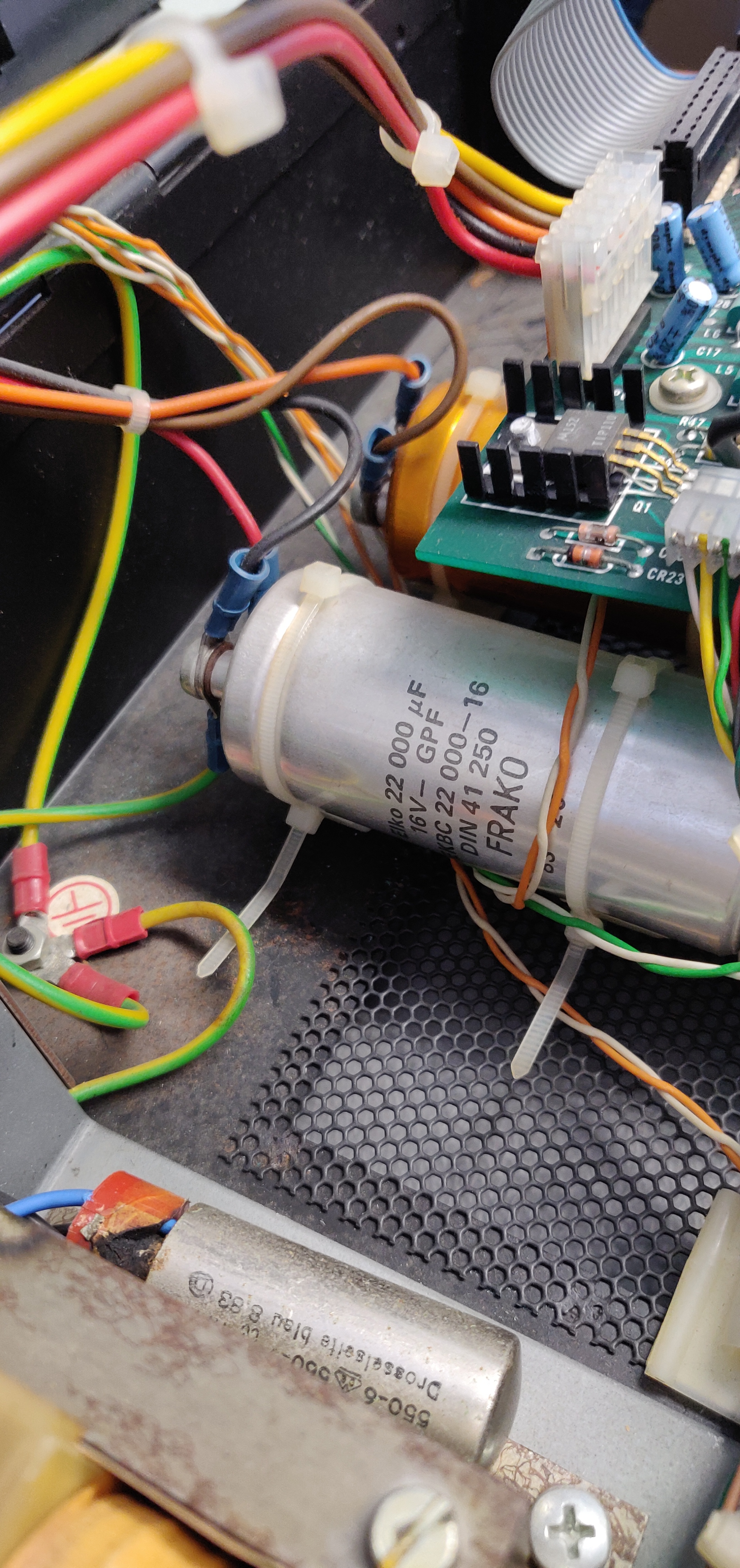
The power supply is a fairly simple design, just a transformer and two very large capacitors:
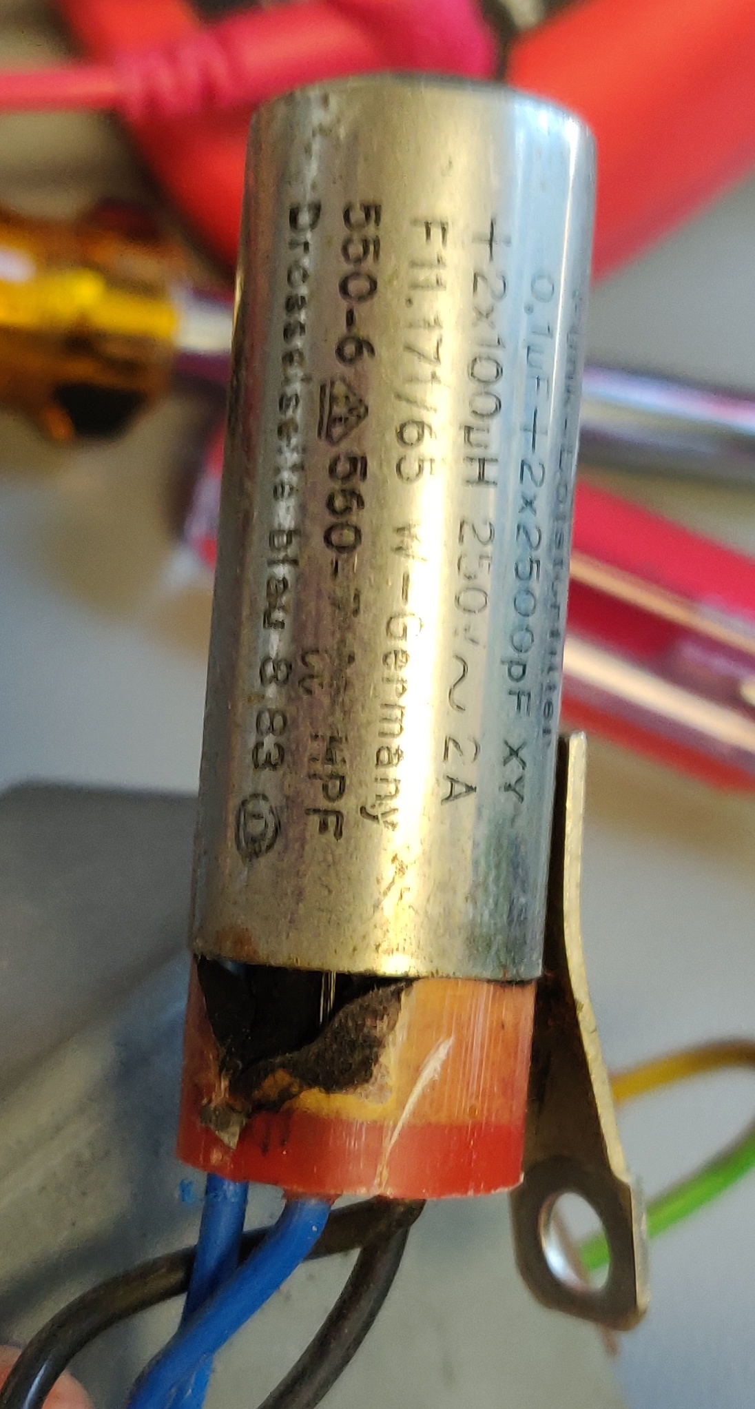
Removing the bad capacitor was enough to get the system up and running again.
Zero-page troubleshooting
After removing the suppression capacitor, the drive would power on, but it immediately started blinking red, indicating a fault. After checking the service guide, I found that the single red blink meant an issue with the zero-page memory (the lowest memory used by the 6502 CPU).
I then connected the logic analyser and I found some interesting results: Although technically the same data was being read back from the memory that was being written, it wasn't actually the correct data. In other words, the memory seemed to work correctly, but somehow the wrong data was being written.
I confirmed this by running the ROM through a disassembler to reverse engineer the self diagnostics routines. The assembly code below is the first step in the 8050's zero-page check for the main CPU. In short, it performs these steps:
- Count from 00 to FF in hexadecimal
- Use this counter as the address and the data, so 00 is written to address 0000, 01 to 0001, etc. etc.
ADDR   HEX        Label     Instruction
----   -----      -----     -----------
F2D9   A2 00                LDX #$00    ; Load register X with value - 00
F2DB   8A         LF2DB     TXA         ; Transfer register X to Accumulator
F2DC   95 00                STA $00,X   ; Store Accumulator in Memory - address 0 + X
F2DE   E8                   INX         ; Increment register X by One
F2DF   D0 FA                BNE LF2DB   ; Branch on Result not Zero - label LF2DB
F2E1   8A         LF2E1     TXA         ; Transfer register X to Accumulator
F2E2   D5 00                CMP $00,X   ; Compare Memory and Accumulator - address 0 + X
F2E4   D0 A7                BNE LF28D   ; Branch on Result not Zero - label F28D
Comparing this to the output of the logic analyser, you can see completely different values being written to RAM. This leaves only one likely option; two chips were active at the same time, creating a bus conflict.
State Number    ADDR    6502 mnemonic                       DATA
____________    ____    ________________________________    ____
46              F2D9      A2   LDX #$00                     A2
47              F2DA      00                                00
48              F2DB      8A   TXA                          8A
49              F2DC      95   memory read                  95
50              F2DC      95   STA $00, x                   95
51              F2DD      00                                00
52              0000      09   memory read                  09
53              0000      09   memory write                 09
54              F2DE      E8   INX                          E8
55              F2DF      D0   memory read                  D0
56              F2DF      D0   BNE $F2DB  (-$06)            D0
57              F2E0      FA                                FA
58              F2E1      8A   memory read                  8A
59              F2DB      8A   TXA                          8A
60              F2DC      95   memory read                  95
61              F2DC      95   STA $00, x                   95
62              F2DD      00                                00
63              0000      09   memory read                  09
64              0001      00   memory write                 00
65              F2DE      E8   INX                          E8
66              F2DF      D0   memory read                  D0
67              F2DF      D0   BNE $F2DB  (-$06)            D0
68              F2E0      FA                                FA
69              F2E1      8A   memory read                  8A
....
2862            F2E0      FA                                FA
2863            F2E1      8A   TXA                          8A
2864            F2E2      D5   memory read                  D5
2865            F2E2      D5   CMP $00, x                   D5
2866            F2E3      00                                00
2867            0000      09   memory read                  09
2868            0000      09   memory read                  09
2869            F2E4      D0   BNE $F28D  (-$59)            D0
On the surface the circuit for triggering the CS (chip select) pins on the ROMs and RIOT (MOS 6532 ICs, which are used as zero-page memory) was very simple, but I couldn't figure out why they used AND gates, which would keep the signals almost always LOW, while the pinout of the 2364 ROMs I found showed them as active LOW. This would mean that the ROMs were almost always active, even at the same time as the RIOTs:
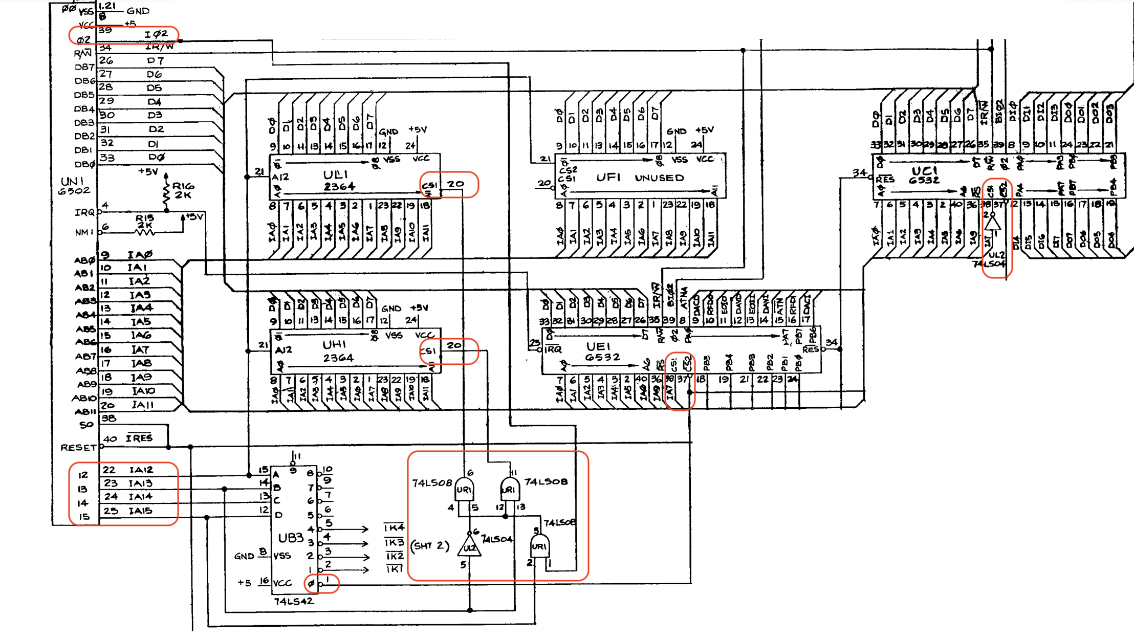
While trying to diagnose the issue further using the logic analyser, I found that the 74LS08 quad AND gate (UR1 in the schematic) had a faulty gate, and I was certain that I had found the cause of the issue.
However, after replacing it, I found that it didn't make any difference at all. And this is the point where I double-checked the 2364 ROM datasheet and found that their CS pin can be programmed to be either active LOW or active HIGH. And obviously they were programmed as active HIGH in this case...
At this point I tested by removing the 2nd ROM chip (UL1) and found that the correct data was now being written and read and this allowed the diagnostics to continue to the next stage.
Unfortunately, this didn't resolve the issue completely, and I had to write a short Python program to check the output of the logic analyzer for memory faults:
with open("print.txt") as file:
    data = file.readlines()


memory = {}
for line in data[6:]:
    address = line[16:20]
    data = line[60:62]
    if line[31:43] == "memory write":
        memory[address] = data
        print(f"{line[0:5]} Successful write at address {address} data: {data}")
    if line[31:42] == "memory read" and address[0:2] == "00" and not data == memory.get(address, "NULL"):
        print(f"{line[0:5]} Memory fault at {address} - Expected data: {memory.get(address)} actual data: {data}")
    elif line[31:42] == "memory read" and address[0] != "F":
        print(f"{line[0:5]} Successful read at address {address} data: {data}")
        pass
Now I could see that on the 2nd stage, address 0004 was returning incorrect data. This was resolved by replacing the RIOT chip in location UC1.
ROM replacement
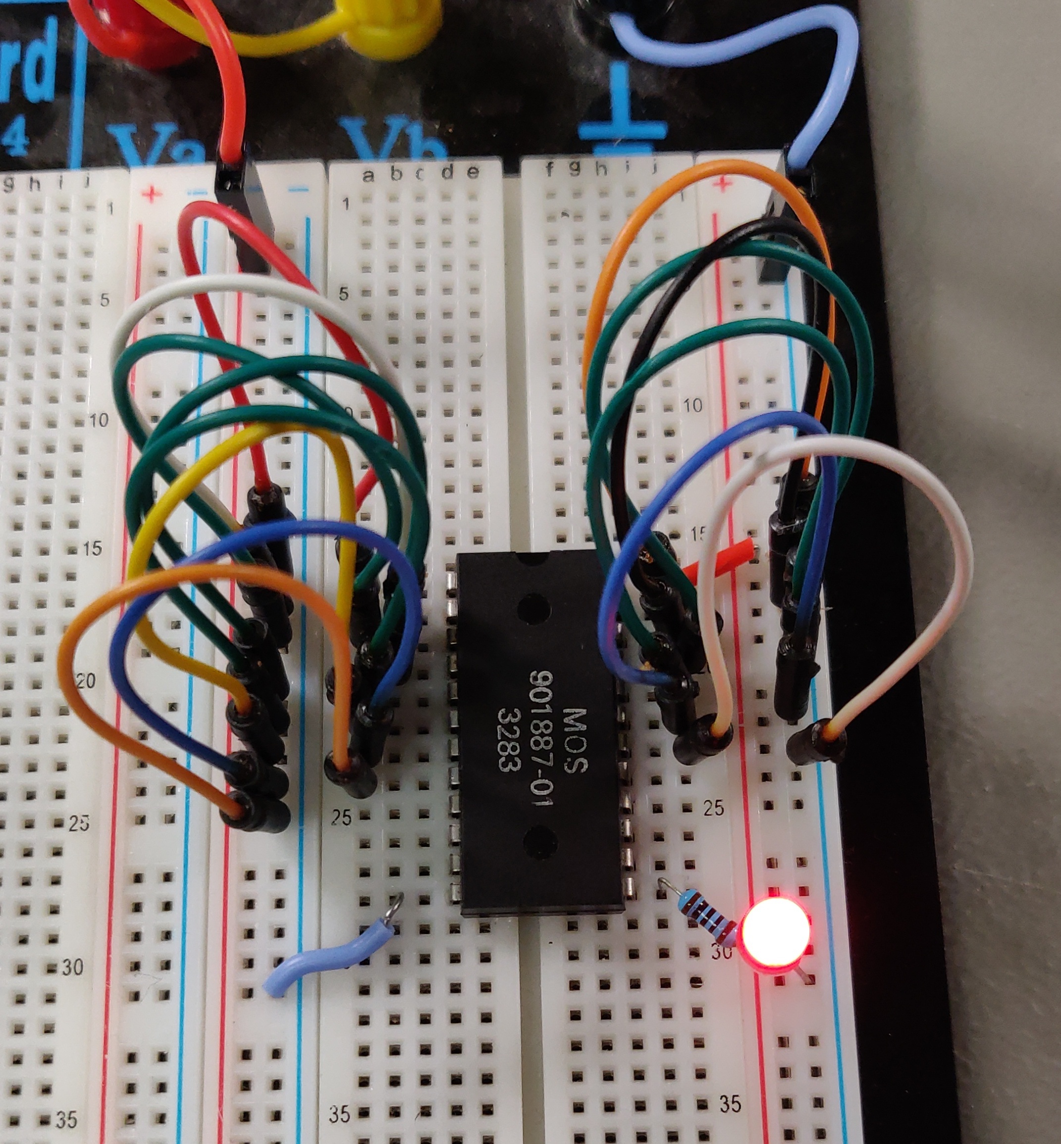
When I tested the ROM on a breadboard, I confirmed that it was driving the data lines regardless of the state of the CS line:
The replacement presented a bit of challenge, the original MOS 2364 ROMs were programmed to be active HIGH, meaning that the IC only drives the data bus when the CS pin is connected to 5v, but the 27C256 EPROM I wanted to replace it with is active LOW, meaning that IC drives the data bus when the CS pin is grounded.
I ended up using a standard adapter board to fit the larger 27C256 IC, but added a 74LS30N (single 8-input AND gate) as an inverter to convert the active HIGH to active LOW:
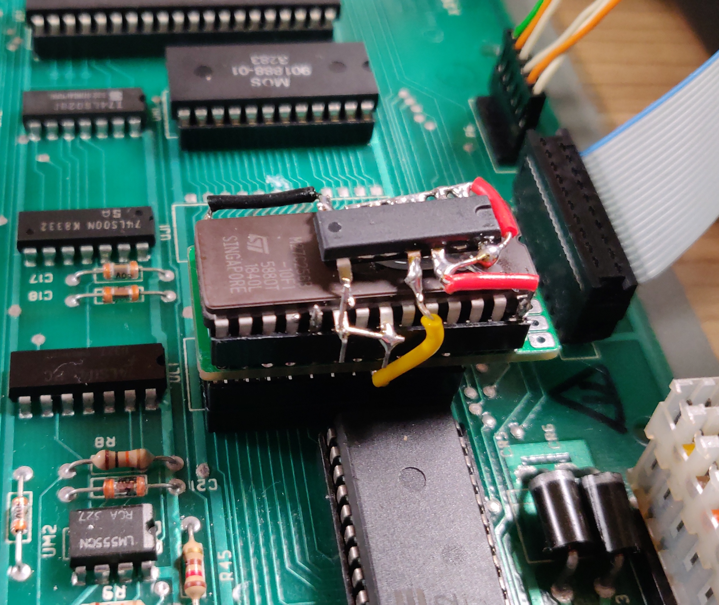
Ideally, this should be replaced with an original Commodore 901887-01 ROM IC.